Home > Products > Communication Module > Optical Fiber RoHS Compliant 100GB /S Cfp2 Er4 40km Optical Transceiver


Optical Fiber RoHS Compliant 100GB /S Cfp2 Er4 40km Optical Transceiver
Product FeaturesSupports up to 112Gbps bit ratesDuplex LC connectorHot pluggableOperating electrical serial data rate up to 27.952493GbpsAPD ROSA4 parallel electrical serial interfaceApplicable for 30km SMF connectionLow power consumption, < 12WDigital Diagnostic Monitor InterfaceMDIO Communicati......
Send Inquiry
Product Description
Product Features
- Supports up to 112Gbps bit rates
- Duplex LC connector
- Hot pluggable
- Operating electrical serial data rate up to 27.952493Gbps
- APD ROSA
- 4 parallel electrical serial interface
- Applicable for 30km SMF connection
- Low power consumption, < 12W
- Digital Diagnostic Monitor Interface
- MDIO Communication Interface
- Compliant with 100GBASE-ER4
- Operating case temperature: Commerical:0 to 70 °C
Applications
- Local Area Network(LAN)
- Wide Area Network(WAN)
- Switch to router interface
Standards
- Compliant with IEEE 802.3ba
- Compliant with CFP2 MSA hardware specifications
- Compliant with CFP2 MSA management specifications
- Compliant with ITU-T G709/Y.1331
- Compliant with RoHS
Functional Description
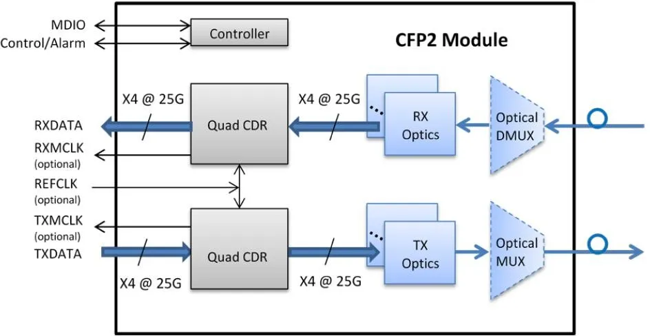
GFC-OLCFXXTXL-CD40, The 100G CFP2 ER4 optical transceiver integrates the transmit and receive path onto one module. On the transmit side, four lanes of serial data streams are recovered, retimed,and passed on to four laser drivers, which control four electric-absorption modulated lasers (EMLs) with 1296, 1300, 1305, and 1309 nm center wavelengths. The optical signals are then multiplexed into a single-mode fiber through an industry-standard LC connector.On the receive side, four lanes of optical data streams are optically demultiplexed by an integrated optical demultiplexer. Each data steam is recovered by a PIN photodetector and transimpedance amplifier, retimed, and passed on to an output driver. This module features a hot-pluggable electrical interface, low power consumption, and MDIO management interface.
Functional Diagram
Absolute Maximum Ratings
Note: Stress in excess of the maximum absolute ratings can cause permanent damage to the transceiver.
Electrical Characteristics
(Tested under recommended operating conditions,unless otherwise noted)
| Parameter | Symbol | Min. | Max. | Unit | Note |
| Supply Voltage | Vcc | -0.5 | 3.6 | V | |
| Storage Temperature | TS | -40 | 85 | °C | |
| Relative Humidity | RH | 0 | 85 | % |
Recommended Operating Conditions
| Parameter | Symbol | Min. | Typ | Max. | Unit | Note |
| Data Rate | DR | 103.2 | 112 | Gb/s | ||
| Supply Voltage | Vcc | 3.14 | 3.3 | 3.46 | V | |
| Operating Case Temp. | Tc | 0 | 70 | °C |
(Tested under recommended operating conditions,unless otherwise noted)
| Parameter | Symbol | Unit | Min | Typ | Max | Notes | ||||
| Voltage Supply Electrical Characteristics | ||||||||||
| Supply Current | Tx Section | Icc | A | 3.75 | 1 | |||||
| Rx Section | ||||||||||
| Power Supply Noise | Vrip | 2% DC | 1MHz | |||||||
| 3% 1 | 10MHz | |||||||||
Total Dissipation | Power | Class1 | Pw | W | 3 | |||||
| Class2 | 6 | |||||||||
| Class3 | 9 | |||||||||
| Class4 | 12 | |||||||||
| Low Power Mode Dissipation | Plow | W | 2 | |||||||
| Inrush Current | Class1 | and | I-inrush | mA/usec | 100 | |||||
| Turn-off Current | Class2 | I-turnoff | mA/usec | -100 | ||||||
| Inrush Current | Class3 | and | I-inrush | mA/usec | 200 | |||
| Turn-off Current | Class4 | I-turnoff | mA/usec | -200 | ||||
| Different Signal Electrical Characteristics | ||||||||
| Single Ended Data Input Swing | mV | 20 | 525 | |||||
| Single Ended Data Output Swing | mV | 180 | 385 | |||||
| Differential Signal Output Resistance | Ω | 80 | 120 | |||||
| Differential Signal Input Resistance | Ω | 80 | 120 | |||||
| 3.3V LVCMOS Electrical Characteristics | ||||||||
| Input High Voltage | 3.3VIH | V | 2.0 | Vcc+0.3 | ||||
| Input Low Voltage | 3.3VIL | V | -0.3 | 0.8 | ||||
| Input Leakage Current | 3.3IIN | uA | -10 | +10 | ||||
| Output HighVoltage (IOH=100uA) | 3.3VOH | V | Vcc-0.2 | |||||
| Output Low Voltage (IOL=100uA) | 3.3VOL | V | 0.2 | |||||
| Minimum Pulse Width of Control Pin Signal | t_CNTL | us | 100 | |||||
| 1.2V LVCMOS Electrical Characteristics | ||||||||
| Input High Voltage | 1.2VIH | V | 0.84 | 1.5 | ||||
| Input Low Voltage | 1.2VIL V | 0.3 | 1.2VIL V | 0.36 | ||||
| Input Leakage Current | 1.2IIN | uA | -100 | +100 | ||||
| Output High Voltage | 1.2VOH | V | 1.0 | 1.5 | ||||
| Output Low Voltage | 1.2VOL | V | -0.3 | 0.2 | ||||
| Output High Current | 1.2IOH | mA | -4 | |||||
| Output Low Current | 1.2IOL | mA | +4 | |||||
| Input Capacitance | Ci | pF | 10 | |||||
High Speed Electrical Characteristics
| Parameter | Symbol | Unit | Min. | Max. | Notes |
| Impedance | Zd | Ω | 90 | 110 | |
| Frequency | MHz | 161.1328125 | 1/64 of electrical lane rate | ||
| Frequency Stability | △f | ppm | -100 | 100 | For Ethernet |
| -20 | 20 | For Telecom | |||
| Differential Voltage | VDIFF | mV | 400 | 900 | Peak to Peak Differential |
| Common mode noise (rms) | mV | 17.5 | |||
RMS jitter | ps | 10 | Random Jitter Over frequency band of 10KHZ<f<10MHZ | ||
| Clock Duty Cycle | % | 40 | 60 | ||
Optical Characteristics
(Tested under recommended operating conditions,unless otherwise noted)
| Parameter | Symbol | Unit | Min | Typ | Max Notes | |
| Optical Transmitter Characteristics | ||||||
| Signaling rate, each lane | GBd | 25.78125 ±100 ppm | 100GBase-ER4 | |||
| 27.9525 ±20 ppm | OTU4 | |||||
| Four Lane Wavelength Range | λ1 | nm | 1294.53 | 1295.56 | 1296.59 | |
| λ2 | 1299.02 | 1300.05 | 1301.09 | |||||
| λ3 | 1303.54 | 1304.58 | 1305.63 | |||||
| λ4 | 1308.09 | 1309.14 | 1310.19 | |||||
| Total launch power | dBm | 8.9 | 100GBase-ER4 | |||||
| Average launch power, each lane | Pavg | dBm | -2.9 | 2.9 | 2 | |||
| Optical modulation amplitude, each lane (OMA)2 | OMA | dBm | 0.1 | 4.5 | ||||
| Difference in launch power between any two lanes (OMA) | dB | 3.6 | ||||||
| Extinction ratio | ER | dB | 8 | 100GBase-ER4 | ||||
| Side-mode suppression ratio | SMSR | dB | 30 | |||||
| Transmitter and dispersion penalty, each lane | TDP | dB | 2.5 | |||||
| Optical return loss tolerance | dB | 20 | ||||||
| Transmitter reflectance3 | dB | -12 | ||||||
| Transmitter eye mask {X1, X2, X3, Y1, Y2, Y3} | {0.25, 0.4, 0.45, 0.25, 0.28, 0.4} | 100GBase-ER4 | ||||||
| Optical Receiver Characteristics | ||||||||
| Receive Rate for Each Lane | Gbps | 25.78125 | 27.9525 | |||||
| Overload Input Optical Power | Pmax | dBm | 5.5 | 3 | ||||
| Average Receive Power for Each Lane | Pin | dBm | -20.9 | 4.5 | 4, 5 | |||
| Receive Power In OMA for Each Lane | PinOMA | dBm | 4.5 | |||||
| Difference in Receive Power in OMA between Any Two Lanes | dBm | 4.5 | ||||||
| Receiver Sensitivity in OMA for Each Lane | SOMA | dBm | -21.4 | 6 | ||||
| Stressed Receiver Sensitivity in OMA for Each Lane | dBm | -17.9 | 7, 8 | |||||
Notes:
- The supply current includes CFP2 module's supply current and test board workingcurrent.
- Average launch power, each lane (min) is informative for 100GBase-LR4, not the principal indicator of signal strength.
- The receiver shall be able to tolerate , without damage, continuous exposure to an optical input signal having this average power level
- The average receive power , each lane (max) for 100GBASE-ER4 is larger than the 100BASE-ER4 transmitter value to allow compatibility with 100BASE-LR4 units at short distances
- Average receive power, each lane (min) is informative and not the principal indicator
- Receiver sensitivity (OMA), each lane (max) is informative
- Measured with conformance test signal at TP3 for BER=10-12
- conditions of stressed receiver sensitivity test: vertical eye closure penalty for each lane is 1.8dB;stressed eye J2 jitter for each lane is 0.3UI; stressed eye J9 jitter for each lane is 0.47UI.

Related Category
Send Inquiry
Please Feel free to give your inquiry in the form below. We will reply you in 24 hours.